
Scientists at ETH Zurich have pioneered a novel method to steer electron dynamics within materials by employing engineered crystal lattices. Utilizing moiré patterns generated through the subtle twisting of atomically thin layers, they successfully influenced electron activity in an adjacent semiconductor layer without physically altering it.
A New Approach to Studying Electron Interactions
Electrons are fundamental to a material’s electrical and magnetic characteristics, but their natural interactions are often subtle and challenging to detect. To enhance these interactions, researchers fabricate artificial crystal lattices with expanded lattice spacing, which reduces electron mobility and heightens interaction effects.
Historically, moiré materials—constructed by layering atomic sheets with slight misalignments—have served this purpose. Although efficient, this approach inherently modifies the physical attributes of the host material, complicating electron interaction analysis.
The innovative strategy from ETH Zurich overcomes these drawbacks by placing the moiré lattice remotely, generating an electric field that modulates electron behavior in a separate semiconductor layer.

Manipulating Electron Patterns via Twisted Boron Nitride
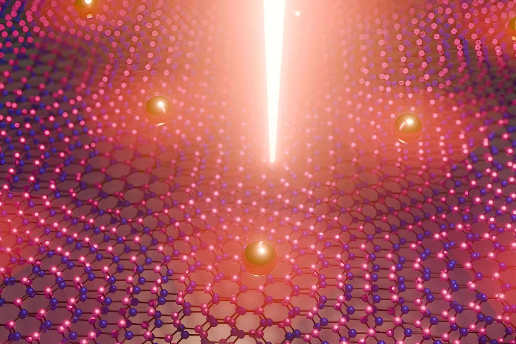
The team, headed by Ataç Imamoğlu, employed two stacked sheets of hexagonal boron nitride (h-BN), a substance rivaling diamond in hardness. By twisting these layers by less than two degrees, they created a spatially periodic electric field that projects beyond the material’s surface.
Positioned beneath this twisted structure was a slender film of molybdenum diselenide (MoSe₂), a semiconductor renowned for its distinctive electronic traits.
The generated electric field influenced the electrons in the MoSe₂, causing them to form an artificial crystal lattice. Unlike conventional moiré materials, this configuration allows researchers to examine electron behavior in a cleaner environment without introducing extraneous physical modifications.
Employing Excitons to Reveal Electron Arrangement
To monitor electron configuration within this lattice, the group utilized excitons — neutral electron-hole pairs formed during light absorption at specific energies. Their lack of charge means they are unaffected by the periodic electric field, making excitons excellent tools for probing electron behavior.
By tuning the applied electric voltage on the semiconductor, researchers controlled the electron density at lattice sites, observing that electrons self-arranged into ordered patterns when filling either one-third or two-thirds of the locations.
Advancing Understanding of Superconductivity Phenomena
Deciphering electron interactions is critical to unraveling the mechanisms behind high-temperature superconductors—materials capable of zero-resistance electricity flow. This cutting-edge technique offers promising avenues to explore how insulating materials become superconducting as electrons are added.
Besides superconductivity, the method’s precision opens new pathways for investigating electron interactions in other quantum materials. By varying the electric field intensity, scientists may eventually uncover exotic phases like chiral spin liquids, a theoretical state yet to be experimentally observed.
- Categories:
- Physics


0 comments
Sign in to Comment